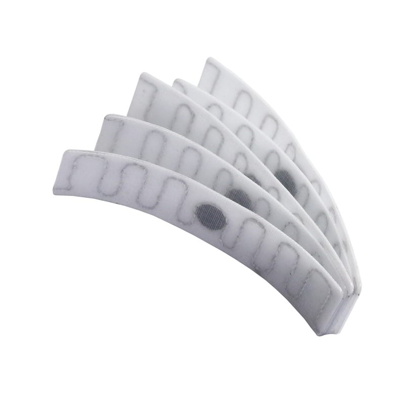
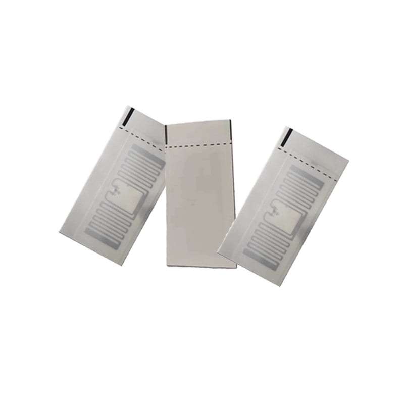
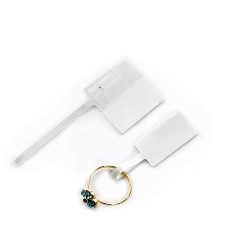
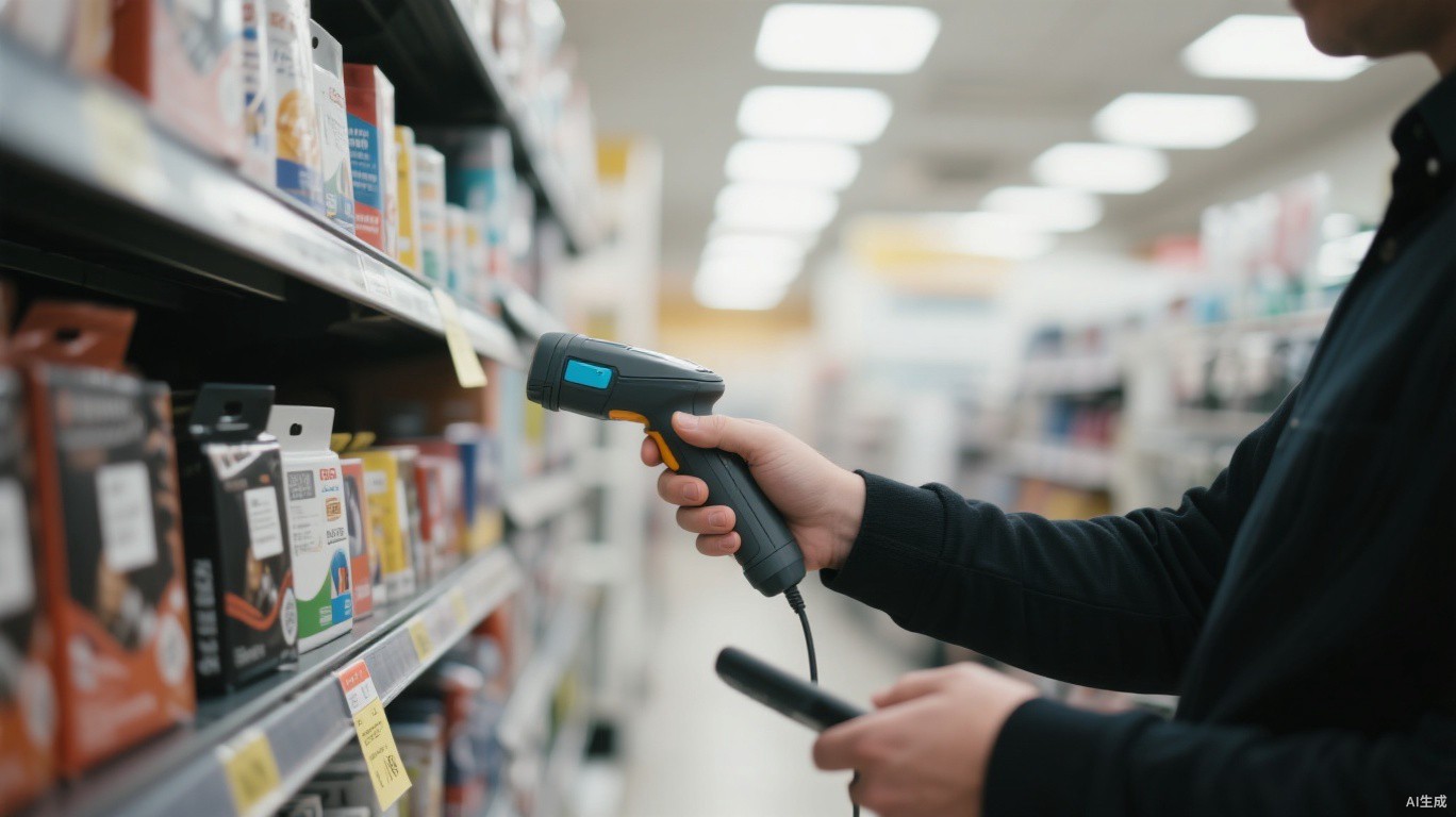
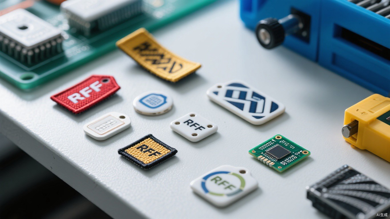
A UHF RFID chip is, physically, a small piece of silicon with a radio attached to it. Everything about the tag — its cost, its read range, the products it can disappear into — is downstream of how small that silicon can be made while still working.
The last five years moved the bare die from roughly 0.4 square millimetres to about 0.18, and the packaged part from three millimetres square to two, with one-millimetre-class devices moving from conference papers into catalogues. That sounds like an incremental process story. It is actually the reason jewellery, medical devices and embedded assets became addressable at all.
The three forces behind smaller chips
Miniaturisation is pulled by cost, pushed by scenarios and constrained by physics.
- Cost: die area is the wafer's currency, and halving the area more than doubles the dies per wafer.
- Scenario: a jewellery tag, a surgical instrument or a power tool housing has no room for a three-millimetre package.
- Physics: a smaller die has lower parasitic capacitance, which helps the front end if the antenna is designed for it.
- Assembly: flip-chip and wafer-level packaging remove the lead frame, which is where much of the package size actually lives.
- Standards: EPC Gen2 and RAIN conformance tests do not relax with die size, so the bar for a new chip is fixed.
From 3 mm to 2 mm: what actually changed
The generational jump was not only an area reduction; it was a sensitivity and memory story.
- The previous mainstream generation sat around 0.4 square millimetres of die, packaged at roughly three by three millimetres.
- The current generation moved to about 0.18 to 0.22 square millimetres, packaged near two by two.
- Read sensitivity improved at the same time, which matters more than area for real deployments.
- User memory grew, allowing a small service record to live on the tag rather than in a database.
- The change that matters most for product design is the pad pitch: it sets the antenna connection geometry, not the die.
The impedance paradox of a tiny die
Smaller is not automatically better at radio frequency, and the datasheet rarely says so.
- Die impedance rises as the device shrinks, so the antenna must be re-matched or range falls.
- A tiny die has less capacitance to work with, which narrows the matching bandwidth.
- Narrow bandwidth makes the tag more sensitive to the material it sits on, not less.
- Read range is set by the power the chip needs to wake up, not by its area; sensitivity is the real specification.
- A chip thirty percent smaller but one decibel less sensitive is a worse product for most logistics use.
Antenna design when the chip is smaller than the pad
The antenna is now the largest part of the tag, and it is where miniaturisation actually stops.
- At 900 MHz the wavelength is about 33 centimetres, so every practical tag antenna is a compromise structure.
- A smaller pad pitch allows a more compact loop, but loop area is also what couples to the reader field.
- For jewellery and medical use the antenna often wraps the item, so the item becomes part of the design.
- Conductive materials detune the antenna, and a ferrite layer adds thickness that may exceed the chip's savings.
- The practical limit is not the chip but the read point: below a certain size only a near-field reader works.
Assembly: wafer-level packaging and the cost curve
The packaging step is where size and price are actually decided.
- Wafer-level packaging keeps the die in wafer form through test and bumping, avoiding per-die handling.
- Flip-chip attach with anisotropic adhesive replaces wire bonding, removing loop height and lead frame.
- The tag cost curve flattens as assembly and antenna dominate; silicon is no longer the main line item.
- Test cost per die does not fall with area, so yield economics improve more slowly than area economics.
- At very high volume the limiting factor becomes handling and placement, not the wafer.
Where a 1 mm tag changes the product, not just the label
The interesting cases are the ones where the tag disappears into the object's construction.
- Jewellery: a tag inside a clasp or a setting, invisible to the customer and surviving daily wear.
- Medical: instrument-level identity that survives autoclave cycles without a visible bump.
- Tools and power equipment: identity moulded into the housing rather than stuck on the outside.
- Consumables and cosmetics: a tag under a label that cannot be peeled off and moved to another item.
- Documents and credentials: a tag thin enough to sit between paper layers without a detectable bulge.
The read-range penalty nobody puts on the datasheet
Every miniaturisation claim should be read alongside the conditions in which it was measured.
- Published sensitivity is measured on a reference antenna in an anechoic chamber, not on the customer's product.
- A tag embedded in metal or liquid may lose more range than it gained from the smaller die.
- Orientation matters more for compact antennas, because the radiation pattern becomes less uniform.
- The vendor's read range usually means best-case orientation at maximum permitted power.
- Re-measure on the actual item, at the actual read point, before committing to a design.
Qualification tests for a chip you can barely see
Smaller devices are harder to inspect, which changes what quality assurance can even mean.
- Visual inspection is no longer a meaningful incoming check; electrical and RF tests carry the burden.
- The assembly adhesive becomes a reliability item, because thermal cycling can delaminate a bump you cannot see.
- ESD sensitivity increases with thinner die, so handling specifications must be enforced rather than assumed.
- Tag-level failure analysis needs decapsulation, so batch sampling replaces unit inspection.
- Keep a golden sample of each lot and measure sensitivity drift over the first year of storage.
A one-millimetre chip is not a novelty. It is the point at which the tag stops being a label stuck on a product and becomes part of the product's design — and that shift moves the decision from the packaging engineer to the product engineer.