A passive UHF inlay is an antenna problem before it is a silicon problem. The chip is a well-behaved, well-documented integrated circuit; the antenna is a piece of aluminium a few micrometres thick, glued to a face sheet, sitting on whatever the user decides to stick it to. That last variable is why identical chips deliver wildly different performance in the field.
The design goal is narrower than it sounds: deliver enough power to the chip's rectifier to wake it, and return a modulated signal strong enough for the reader to decode, at every frequency the reader is allowed to use, on the object it will actually be attached to.
What does the chip actually look like to the antenna?
A Gen2 chip is not a 50-ohm load. At the frequencies of interest its input impedance is a large capacitive reactance in series with a small resistance — commonly quoted as roughly 12 to 20 ohms real, minus 100 to 250 ohms imaginary, depending on frequency and chip family. A representative value used throughout the industry is 12 - j140 ohms.
Two consequences follow immediately. First, the antenna cannot be borrowed from classical 50-ohm design tables; it must be designed to present the complex conjugate, roughly 12 + j140 ohms, at the tag's operating frequency. Second, matching network losses matter, because the impedance transformation ratio is large and any resistive loss in the match sits directly in the power path.
- Match the conjugate, not 50 ohms. A tag antenna measured at 50 ohms is being measured wrong.
- Every chip generation changes the target. Design files are chip-specific, not generic.
- Sensitivity improves as the chip's real impedance falls, so newer chips are easier to feed.
Why is the dipole still the default?
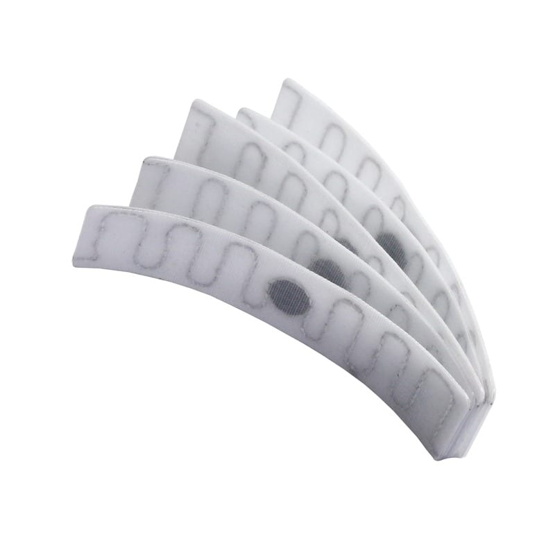
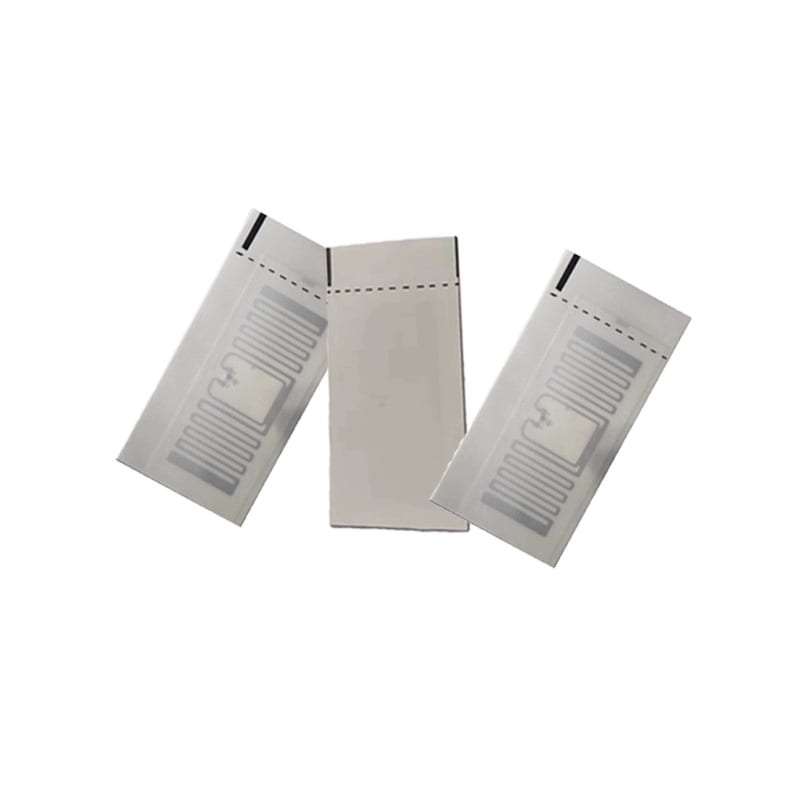
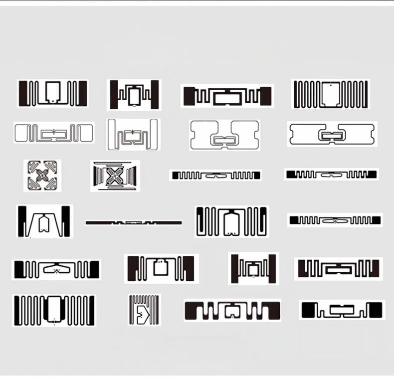
The half-wave dipole is the reference structure for label tags because it is simple, cheap, and naturally balanced. Printed on PET foil with a meandered arm it fits inside a 70 by 20 mm label while keeping the electrical length required for resonance.
Its weakness is bandwidth. A thin dipole matched to a high-Q chip covers perhaps 20–40 MHz at UHF, which is enough for one region and not enough for a global SKU. That is why most modern inlays add a T-match or inductive loop: it transforms the impedance and broadens the response, at the cost of some gain and some sensitivity to nearby material.
- Best for: cartons, apparel labels, paper documents, general logistics.
- Gain: 1.5–2.2 dBi typical, nearly omnidirectional in the tag plane.
- Practical limit: mounting directly on a large metal surface detunes it completely.
When does a patch or microstrip antenna make sense?
A patch antenna is a resonant cavity: a metal patch over a ground plane separated by a dielectric. Because the ground plane shields the radiating structure from whatever is behind it, a patch is the natural choice for on-metal tags. It is also naturally directional, which is useful when you want to read one side of an asset and ignore the other.
The price is physical. A half-wave patch at 915 MHz needs a substrate with a reasonable dielectric constant to stay small, and the ground plane must be electrically continuous and larger than the patch. Typical on-metal tags are 40 by 40 mm to 100 by 50 mm rigid PCBs with a foam or rigid spacer.
- Best for: metal tools, containers, machine parts, IT assets, returnable metal pallets.
- Gain: 3–6 dBi, with a defined beam and a defined back lobe.
- Cost: 5–20 times a paper label, and it will not survive a wash cycle unless encapsulated.
What does broadband actually buy you?
A tag sold globally must work from 865 to 928 MHz and, in some markets, up to 960 MHz. That is a 10 % fractional bandwidth requirement, which is demanding for a small, high-Q structure.
Three techniques are used in practice. A T-match or double-T match provides a second resonance that broadens the band. Meandered arms with varying line width distribute the current and flatten the response. A small parasitic element or a slot can be added to shape the impedance locus so the tag stays matched at both band edges.
- Broadband tags usually lose 0.5–1 dB of peak gain compared with a narrowband design.
- They are the right default for any SKU shipped across regions.
- A broadband tag is not a metal tag: different problem, different structure.
How do size, gain and bandwidth trade against each other?
Physics sets a floor on size. A resonant antenna at 900 MHz wants to be roughly 80–160 mm long in free space; meandering folds it into a smaller footprint but narrows bandwidth and lowers radiation resistance, which makes matching harder and losses more visible.
- Smaller tag: narrower band, lower gain, more sensitive to the object behind it.
- Larger tag: more gain, wider band, but physically incompatible with small items.
- Higher dielectric constant substrate: shrinks the tag, concentrates the field, and increases loss.
The practical rule is to never shrink below the size where the tag still reads at the distance the process requires, with a 3–6 dB margin for real-world losses.
What do the substrate and the object behind the tag do?
Every tag is a two-part system: the inlay and its immediate environment. The environment is not a detail; it is half the design.
- Water and human tissue: high dielectric constant, absorb UHF energy, detune the antenna downward.
- Metal: reflects the field, shorts the dipole arms if mounted directly, and shifts resonance.
- Glass and plastic: mild detuning, usually handled by a small offset from the surface.
- Foam or corrugated cardboard: low loss, close to free space, the easiest substrate.
The standard remedies are a foam standoff of 3–10 mm, a ferrite backing layer that isolates the antenna from metal, or a rigid bracket that turns the metal into part of the antenna. Each adds cost and thickness, and each must be validated on the actual product, not on a test card.
How do you choose and test a tag antenna in practice?
Start from the object and the read distance, then work backwards. The order that avoids expensive mistakes is: object material, required read distance, reader power and antenna, region, then inlay.
- Test on the real product, in the real orientation, with the real reader.
- Measure read rate over 100 passes minimum, and record the distribution, not the average.
- Test the worst orientation explicitly — a pallet corner, a folded garment edge, a tag facing away from the antenna.
- Keep a control tag of known performance to separate reader problems from tag problems.
If a candidate inlay reads at 4 metres on cardboard and 30 centimetres on the metal container, the inlay is fine and the application is wrong. That distinction is the whole discipline of tag antenna selection.
Bottom line
Design the match to the chip's complex conjugate, expect the dipole to be the default and the patch to be the metal solution, choose broadband for any multi-region SKU, and treat the object behind the tag as part of the antenna. Most RFID performance problems that look like reader failures are antenna problems wearing a different hat.